Digital Diagnostic Functions
BT-SFP-10G10 transceivers support the 2-wire serial communication protocol as defined in the SFP+ MSA.
The standard SFP serial ID provides access to identification information that describes the transceiver’s capabilities, standard interfaces, manufacturer, and other information.
Additionally, SFP+ transceivers provide a unique enhanced digital diagnostic monitoring interface, which allows real-time access to device operating parameters such as transceiver temperature, laser bias current, transmitted optical power, received optical power and transceiver supply voltage. It also defines a sophisticated system of alarm and warning flags, which alerts end-users when particular operating parameters are outside of a factory set normal range.
The SFP MSA defines a 256-byte memory map in EEPROM that is accessible over a 2-wire serial interface at the 8 bit address 1010000X (A0h).The digital diagnostic monitoring interface makes use of the 8 bit address 1010001X (A2h), so the originally defined serial ID memory map remains unchanged.
The operating and diagnostics information is monitored and reported by a Digital Diagnostics Transceiver Controller (DDTC) inside the transceiver, which is accessed through a 2-wire serial interface. When the serial protocol is activated, the serial clock signal (SCL, Mod Def 1) is generated by the host. The positive edge clocks data into the SFP transceiver into those segments of the E2PROM that are not write-protected. The negative edge clocks data from the SFP transceiver. The serial data signal (SDA, Mod Def 2) is bi-directional for serial data transfer. The host uses SDA in conjunction with SCL to mark the start and end of serial protocol activation. The memories are organized as a series of 8-bit data words that can be addressed individually or sequentially.
Host – Transceiver Interface Block Diagram

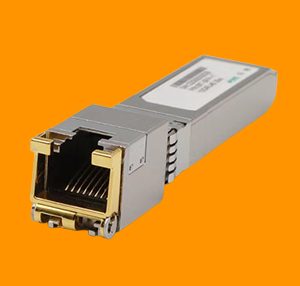
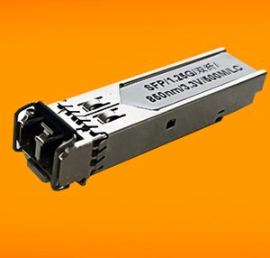
Outline Dimensions
 Regulatory Compliance
| Feature |
Reference |
Performance |
| Electrostatic discharge(ESD) |
IEC/EN 61000-4-2 |
Compatible with standards |
| Electromagnetic Interference (EMI) |
FCC Part 15 Class B EN 55022 Class B (CISPR
22A) |
Compatible with standards |
| Laser Eye Safety |
FDA 21CFR 1040.10, 1040.11 IEC/EN 60825-1, 2 |
Class 1 laser product |
| Component Recognition |
IEC/EN 60950, UL |
Compatible with standards |
| ROHS |
2002/95/EC |
Compatible with standards |
| EMC |
EN61000-3 |
Compatible with standards |
")


Reviews
There are no reviews yet.